|
|
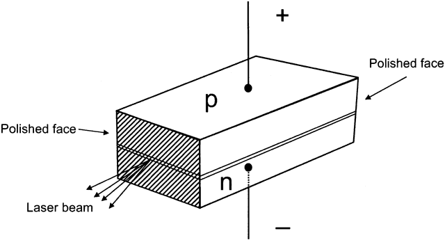
| Fig. 7. Here, n-type and p-type semiconductors are joined at the junction. Negative charge is applied to the n-type side, positive charge to the p-type side. The back is mirrored and the front is partially mirrored to allow laser emission. The sides are roughened to prevent laser emission in other directions. |